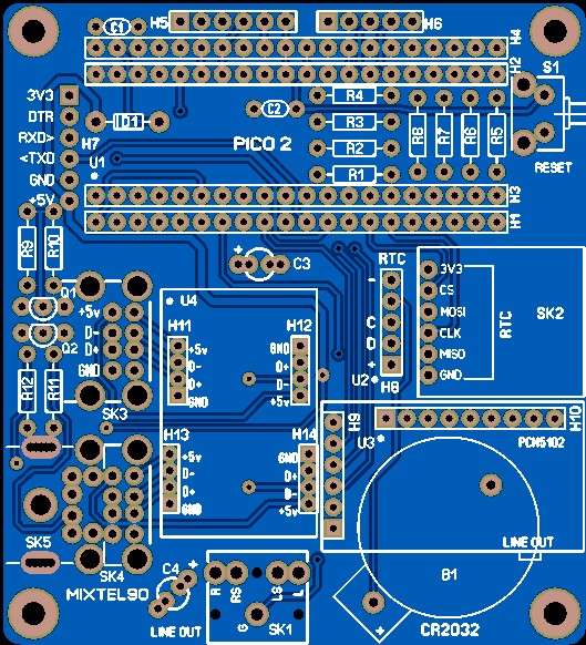
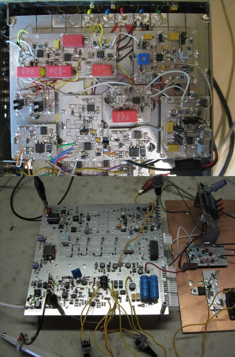
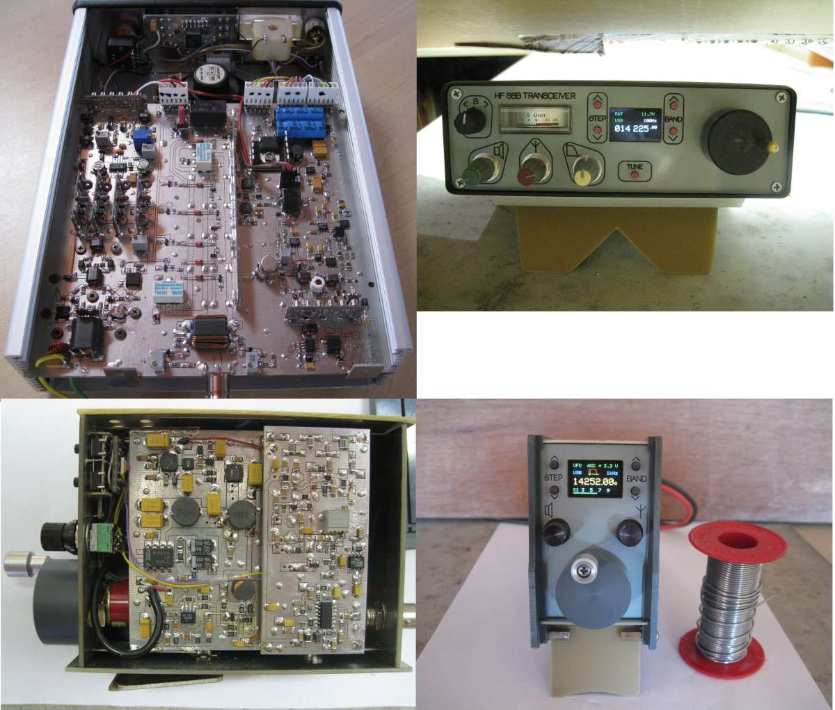
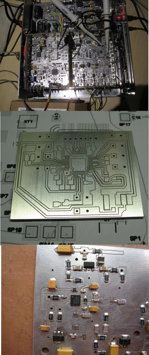
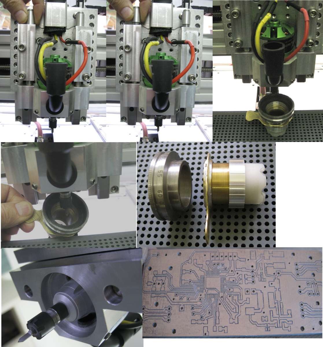
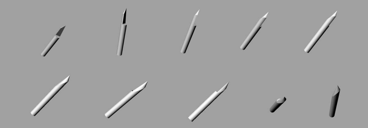
Isolation milling of PCBs
Isolation milling of PCBs
- This topic has 14 replies, 8 voices, and was last updated 19 December 2025 at 19:13 by
 umbriago.
- Please log in to reply to this topic. Registering is free and easy using the links on the menu at the top of this page.
Latest Replies
-
- Topic
- Voices
- Last Post
-
-
Mechanical lubrication steam locos. Non return valve opening pressure
Started by:
peter allen 1
in: General Questions
- 2
-
19 July 2026 at 05:59
Speedy Builder5
-
Honing cylinder
Started by:
Speedy Builder5
in: Workshop Techniques
- 4
-
19 July 2026 at 05:56
Diogenes
-
Bridgeport Series 1 CNC
1
2
3
Started by:
tomcnc
in: CNC machines, Home builds, Conversions, ELS, automation, software, etc tools
- 12
-
19 July 2026 at 02:22
seemack
-
Interactive article on Beam Engines
Started by:
glinscott
in: Stationary engines
- 3
-
18 July 2026 at 23:52
glinscott
-
Face Drive Pins
Started by:
Michael Gilligan
in: Materials
- 3
-
18 July 2026 at 22:40
ega
-
Steam Loco component interconnection diagram
Started by:
Trevor Wood 6
in: Beginners questions
- 2
-
18 July 2026 at 22:22
noel shelley
-
New comer
Started by:
vgvikram171
in: Introduce Yourself – New members start here!
- 1
-
18 July 2026 at 20:43
vgvikram171
-
Fixturing conundrum with Hemingway die filer kit
Started by:
timdotd
in: Workshop Techniques
- 6
-
18 July 2026 at 18:52
timdotd
-
Use of insert type lathe tools
1
2
Started by:
JA
in: Workshop Tools and Tooling
- 16
-
18 July 2026 at 18:39
JA
-
Help ID’ing Round Carbide Insert and Finding a Supplier
1
2
Started by:
Jon Gibbs
in: Workshop Tools and Tooling
- 10
-
18 July 2026 at 18:07
renardiere7
-
Plug in Solar
1
2
3
4
Started by:
Vic
in: The Tea Room
- 26
-
18 July 2026 at 17:03
Macolm
-
Smart & Brown model A spindle lock
Started by:
old mart
in: Workshop Tools and Tooling
- 2
-
18 July 2026 at 16:56
Steve101
-
Links for Workshop and Model Engineering STLs and other files.
Started by:
Neil Wyatt
in: 3D Printers and 3D Printing
- 10
-
18 July 2026 at 16:29
Mark Rand
-
Pipe Size Puzzle.
Started by:
Nigel Graham 2
in: Locomotives
- 6
-
18 July 2026 at 14:52
Zan
-
Nut screws washer and bolts – you know the old joke
Started by:
Kiwi Bloke
in: General Questions
- 13
-
18 July 2026 at 14:47
duncan webster 1
-
Myford VMC Spindle Advice Please.
1
2
3
Started by:
Nigel Graham 2
in: Manual machine tools
- 12
-
18 July 2026 at 11:59
Graham Meek
-
Small 3D Metal Printed Part
Started by:
Julie Ann
in: 3D Printers and 3D Printing
- 1
-
18 July 2026 at 11:43
Julie Ann
-
Help please! Workshop clearance
1
2
Started by:
ksw
in: General Questions
- 12
-
18 July 2026 at 10:34
bernard towers
-
QCTP
1
2
Started by:
James A
in: Workshop Tools and Tooling
- 20
-
18 July 2026 at 09:12
James A
-
New project for 2025
1
2
Started by:
SteveP
in: I/C Engines
- 8
-
17 July 2026 at 21:58
SteveP
-
Very Low Q
Started by:
duncan webster 1
in: Clocks and Scientific Instruments
- 2
-
17 July 2026 at 18:39
John Haine
-
How Good Are 3D Printers?
1
2
Started by:
Neil Wyatt
in: 3D Printers and 3D Printing
- 19
-
17 July 2026 at 17:17
Roderick Jenkins
-
My adventures with a bench top CNC mill
1
2
3
Started by:
John Hinkley
in: CNC machines, Home builds, Conversions, ELS, automation, software, etc tools
- 8
-
17 July 2026 at 16:13
JasonB
-
Maisie
Started by:
ian Holdsworth
in: Beginners questions
- 10
-
17 July 2026 at 12:48
KenL
-
My Intro
Started by:
Martin Freestone
in: Introduce Yourself – New members start here!
- 6
-
17 July 2026 at 11:42
Howard Lewis
-
Mechanical lubrication steam locos. Non return valve opening pressure
Latest Issue
Newsletter Sign-up
Latest Replies
- Mechanical lubrication steam locos. Non return valve opening pressure
- Honing cylinder
- Bridgeport Series 1 CNC
- Interactive article on Beam Engines
- Face Drive Pins
- Steam Loco component interconnection diagram
- New comer
- Fixturing conundrum with Hemingway die filer kit
- Use of insert type lathe tools
- Help ID’ing Round Carbide Insert and Finding a Supplier