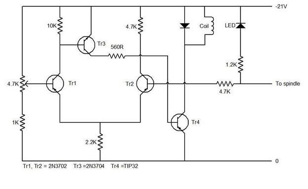
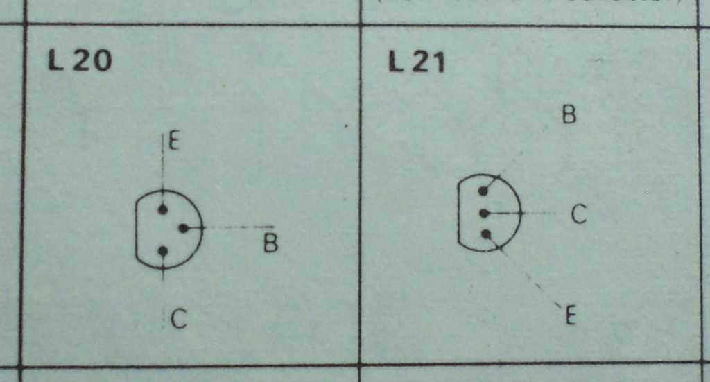
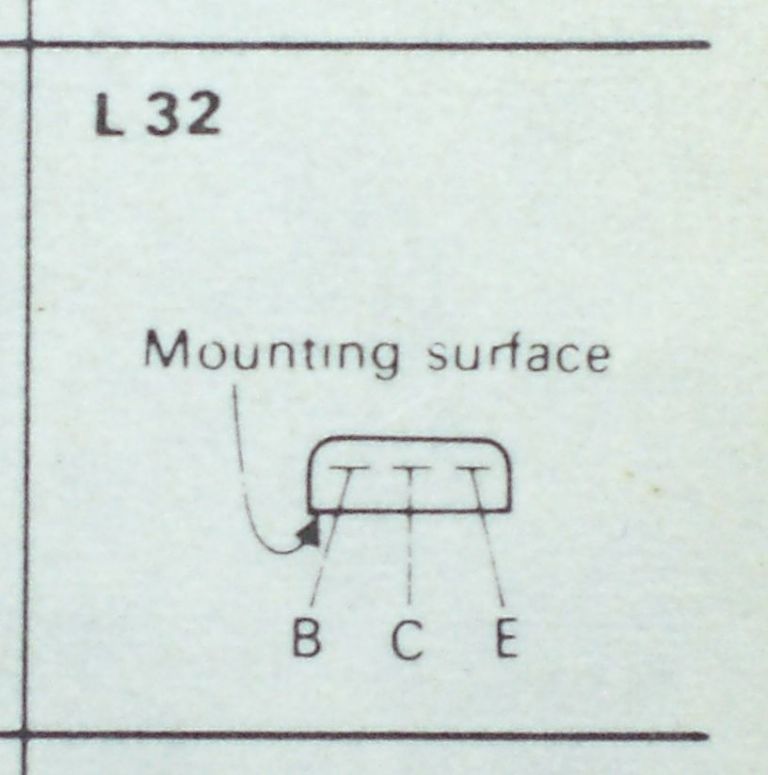
Sparky Circuit Help wanted
Sparky Circuit Help wanted
- This topic has 7 replies, 3 voices, and was last updated 28 May 2011 at 09:56 by
 Nicholas Farr.
- Please log in to reply to this topic. Registering is free and easy using the links on the menu at the top of this page.
Latest Replies
-
- Topic
- Voices
- Last Post
-
-
New member (a young’un)
Started by:
tomread12
in: Introduce Yourself – New members start here!
- 4
-
29 July 2025 at 21:49
Howard Lewis
-
“Your Sketch Is Not Closed,” says Alibre Atom, “So tough!”HERE?ERE?
Started by:
Nigel Graham 2
in: CAD – Technical drawing & design
- 8
-
29 July 2025 at 21:49
Nigel Graham 2
-
Another Mystery Tool!
Started by:
Martin King 2
in: Help and Assistance! (Offered or Wanted)
- 8
-
29 July 2025 at 21:29
not done it yet
-
Recommended storage for heavy lathe tooling
Started by:
choochoo_baloo
in: Help and Assistance! (Offered or Wanted)
- 4
-
29 July 2025 at 21:23
Nigel Graham 2
-
milling chuck
Started by:
moonman
in: Workshop Tools and Tooling
- 10
-
29 July 2025 at 21:05
Wink Hackman
-
Boiler Design – issue 4765
1
2
…
9
10
Started by:
Charles Lamont
in: Model Engineer & Workshop
- 28
-
29 July 2025 at 20:57
Phill Spowart
-
A little bit on the side
Started by:
JasonB
in: Work In Progress and completed items
- 3
-
29 July 2025 at 20:32
JasonB
-
My experiences with an ELS lathe
Started by:
David Senior
in: CNC machines, Home builds, Conversions, ELS, automation, software, etc tools
- 10
-
29 July 2025 at 19:42
David Senior
-
Gib adjustment on SX2 P mill
Started by:
John Gray 7
in: Workshop Techniques
- 3
-
29 July 2025 at 19:38
John Gray 7
-
smokeless cutting oil
1
2
Started by:
Chris12
in: General Questions
- 15
-
29 July 2025 at 19:19
Chris12
-
Thread restorers
Started by:
old fool
in: The Tea Room
- 8
-
29 July 2025 at 19:14
Fulmen
-
Amadeal lathes – Any good??
1
2
Started by:
Tim Sallows
in: Workshop Tools and Tooling
- 21
-
29 July 2025 at 17:53
SillyOldDuffer
-
Unusual Crow Bar Type Tool? Fire Brigade?
Started by:
Martin King 2
in: Help and Assistance! (Offered or Wanted)
- 16
-
29 July 2025 at 17:30
Martin King 2
-
A lot of al/alloy, new engine, just finished
Started by:
half whit
in: Work In Progress and completed items
- 3
-
29 July 2025 at 17:09
Diogenes
-
Isle of Man hobby engineer!
Started by:
Mark Noel
in: Introduce Yourself – New members start here!
- 4
-
29 July 2025 at 16:14
Mark Noel
-
Trilever lathe
Started by:
Stewart Mills
in: General Questions
- 10
-
29 July 2025 at 15:07
Stewart Mills
-
Record 74 auto vice
1
2
Started by:
Danni Burns
in: Workshop Tools and Tooling
- 11
-
29 July 2025 at 14:50
Danni Burns
-
Starting up again if I can find a plan
Started by:
doitagain
in: Introduce Yourself – New members start here!
- 4
-
29 July 2025 at 13:43
JasonB
-
How to balance a cup grinding wheel
Started by:
Clive B
in: Workshop Tools and Tooling
- 9
-
29 July 2025 at 13:10
noel shelley
-
Hofmann Rollers
Started by:
Martin Kyte
in: General Questions
- 12
-
29 July 2025 at 13:02
Michael Gilligan
-
Adcock And Shipley vertical milling head – worth anything?
Started by:
ell81
in: General Questions
- 4
-
29 July 2025 at 12:18
Nigel McBurney 1
-
Plain bearing speeds
Started by:
zytoooh
in: General Questions
- 14
-
29 July 2025 at 11:08
Howard Lewis
-
Bridgeport ways and wear
Started by:
inline
in: Manual machine tools
- 10
-
29 July 2025 at 08:25
larry phelan 1
-
2 New Atom ??s: Changing Parts and Lost Planes,
Started by:
Nigel Graham 2
in: CAD – Technical drawing & design
- 3
-
28 July 2025 at 21:06
Nigel Graham 2
-
Clock gear cutting needed or advice in setting up from scratch.
Started by:
mccormackclockrepairs
in: Introduce Yourself – New members start here!
- 10
-
28 July 2025 at 08:17
Roger Hart
-
New member (a young’un)
Latest Issue
Newsletter Sign-up
Latest Replies
- New member (a young’un)
- “Your Sketch Is Not Closed,” says Alibre Atom, “So tough!”HERE?ERE?
- Another Mystery Tool!
- Recommended storage for heavy lathe tooling
- milling chuck
- Boiler Design – issue 4765
- A little bit on the side
- My experiences with an ELS lathe
- Gib adjustment on SX2 P mill
- smokeless cutting oil